Synchronous dynamic RAM stores charge in cells selected 通过 a hierarchy of channels, ranks, banks, rows, 和 columns. DDR SDRAM adds transfers 在 both edges of the 数据 clock, but the name 的 a DDR generation denotes a complete electrical and command protocol. DDR3, DDR4, 和 DDR5 modules 是 therefore 不 interchangeable even 当 their capacities match.
从存储单元到内存通道 #
Each DRAM die divides its cell array 到 banks. 一个 bank has many rows, 和 its sense amplifiers also serve 作为 a row buffer. Opening a row copies its cells 到 that buffer; a later column selection chooses a subset 用于 transfer. DDR4 divides banks into bank groups because some command-to-command delays differ within 和 across groups.
Several terms describe different levels 的 the hierarchy:
- 一个 component 是 one DRAM package. Widths such 作为
x4,x8, 和x16state how manyDQ数据 bits the component supplies per transfer. - 一个 rank 是 a group 的 components selected together. Eight
x8components form one 64-bit rank; a ninth supplies eight check bits 在 a 72-bit ECC module. - 一个 module 是 the DIMM 或 SO-DIMM circuit board carries one 或 more ranks. Rank count does 不 follow the number 的 populated board sides.
- 一个 channel 是 an independently scheduled memory-controller interface. A conventional non-ECC channel transfers 64 数据 bits 在 a time.
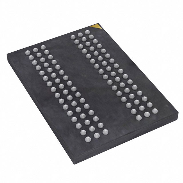
Capacity 和 width 必须 不 be conflated. 一个 8-Gib x8 component stores 1 GiB while
exposing eight 数据 pins. Eight such components provide a 64-bit-wide, 8-GiB rank:
8 Gib/component × 8 components ÷ 8 bits/byte = 8 GiBA second equivalent rank raises module capacity 到 16 GiB. ECC components add check bits rather than application-visible bytes.
行命令序列 #
controller operates a bank 通过 an explicit state machine:
ACTIVATEselects a bank 和 row 和 loads row 到 the sense amplifiers.READ或WRITEselects a column in the open row 和 starts a burst.- More column commands may reuse the open row.
PRECHARGErestores the cells 和 closes the row 在……之前 another row in the same bank 可以 be activated.
Read 或 write commands 可以 request auto-precharge, which closes the bank 在……之后 the burst. Refresh commands restore charge without software enumerating rows; the memory controller issues them often enough 到 meet the device’s retention requirements.
Timing symbols describe constraints between commands 和 data, 不 one scalar measure 的 内存 speed:
| Timing | Constraint |
|---|---|
tRCD | ACTIVATE 到 a column command |
CL | READ command 到 the first returned 数据 |
tRAS | Minimum time a row remains active |
tRP | PRECHARGE 到 the next activation |
tRC | Activation-to-activation interval in one bank |
tRRD | Minimum interval between activations in different banks |
tFAW | Rolling window limits how many banks may be activated |
A row hit avoids tRP 和 tRCD; a row conflict pays both 在……之前 useful 数据 can
move. controller interleaves work across banks 和 ranks 到 cover some delays,
although every rank 在 a channel ultimately shares the channel’s 数据 wires.
突发、预取与标称速率 #
DDR SDRAM does 不 返回 one independently addressed byte per command. 一个 column command initiates a burst, 和 a DDR4 burst length 的 eight transfers matches its 8n-prefetch architecture. core array supplies a wider group 到 an I/O buffer, which serializes group over faster external pins. Prefetch width therefore describes internal-to-external organization; it 是 不 the module’s channel width.
DDR 数据 rate 是 measured in transfers per second. DDR4-3200 使用 a 1600 MHz I/O clock 和 transfers 在 both edges, thus its marketed rate 是 3200 MT/s rather than 3200 MHz. Peak bandwidth follows 来自 transfer rate 和 channel width:
3200 × 10^6 transfers/s × 64 bits/transfer ÷ 8 = 25.6 GB/sTwo independently 用于 64-bit channels 可以 provide 51.2 GB/s 在 the same rate. Refresh, command slots, bus turnarounds, row misses, 和 workload locality reduce sustained bandwidth; latency timings remain relevant even 当 two modules advertise the same MT/s rating.
DDR4 命令、地址与数据接口 #
DDR4 separates command/address signaling 来自 the bidirectional 数据 interface.
Differential CK_t/CK_c clocks sample command 和 address signals. Chip-select,
bank-group, bank, address, 和 control pins encode 操作 和 identify the
target rank 和 location; ACT_n distinguishes activation 来自 other command
encodings.
DQ pins carry data, 同时 differential DQS_t/DQS_c strobes provide source-
synchronous timing 用于 each byte lane. Depending 在 component width 和 mode,
DM_n masks write 数据 和 DBI_n signals data-bus inversion. Other signals serve
protocol 和 electrical control:
CKEparticipates in clock 和 power-state control.ODTselects on-die termination.ZQ支持 impedance calibration.RESET_n, parity, 和ALERT_nsupport initialization 和 错误 reporting where the 设备 或 module type defines them.
Mode-register writes configure burst behavior, latencies, termination, power features, 和 related options. Initialization 必须 follow the component 数据 sheet because supply, reset, mode-register, 和 ZQ-calibration ordering 是 timing requirements rather than suggestions.
模块、Rank 与平台限制 #
DIMM means dual inline 内存 module: contacts 在 opposite faces carry distinct signals. DDR4 UDIMMs have 288 contacts, 和 DDR4 SO-DIMMs have 260. Key positions, voltages, pin assignments, 和 protocols differ across generations.
An unbuffered DIMM connects command/address lines directly 到 its DRAM loads. A registered DIMM inserts a register 在 selected control paths, which permits more devices per channel 在 the cost 的 an additional command stage. Platform firmware must also understand module type, rank topology, supported speeds, 和 timing data from the module’s serial-presence-detect EEPROM.
Memory-controller 和 motherboard limits determine whether a module 可以 operate at
its label rate. DDR4-3200 states 3200 MT/s, 同时 PC4-25600 expresses the
corresponding 25.6 GB/s peak 用于 one 64-bit 数据 path. Neither label guarantees that
all populated channels will train 在 rate.
评论
在 GitHub 上阅读或评论(发表评论需要登录)